PCB Basics
After creating the schematic, you can move on to designing the PCB. Good PCB design minimizes noise, ensures reliable connections, and balances performance with manufacturability. To start with, focus on keeping layouts simple and organized.
Setup
- When laying out the PCB, first ensure that the completed schematic has been validated as necessary.
- If you haven't done so already, you should add a PCB document to the project.
Layers
The Stackup
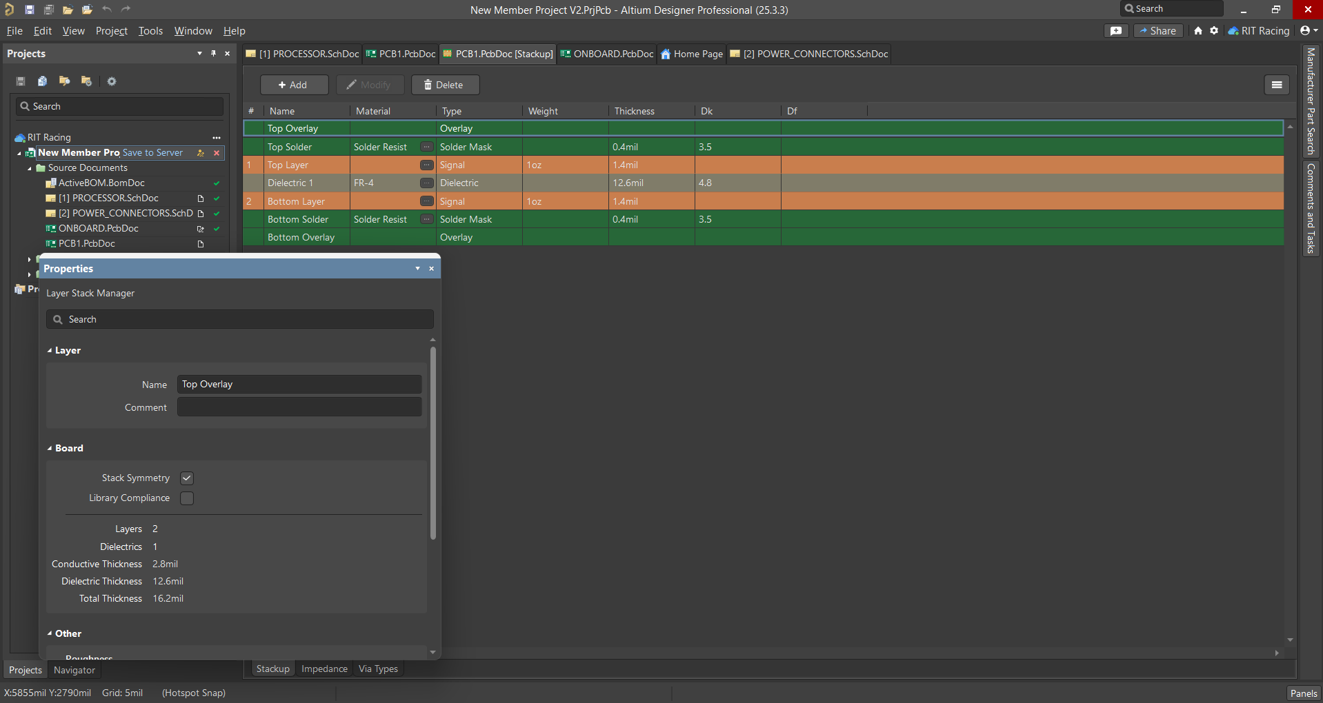
A PCB contains multiple layers, each of which serves a different purpose. The configuration this is known as the layer stackup. The team's PCBs often use 4 layers:
-
Top Layer (Signal) – This is where the main routing and component placement is.
-
Inner Layer 1 (Ground Plane) – A solid ground for signal return paths and EMI (electromagnetic interference) control.
-
Inner Layer 2 (Power Plane) – Distributes power across the circuit (e.g., 5V, 3.3V).
-
Bottom Layer (Signal) – For secondary routing or ground fill; also used for components in dense layouts.
Some boards may require different layer configurations depending on complexity or signal requirements. This should be kept in mind before starting layout.
Access and Edit Layers
-
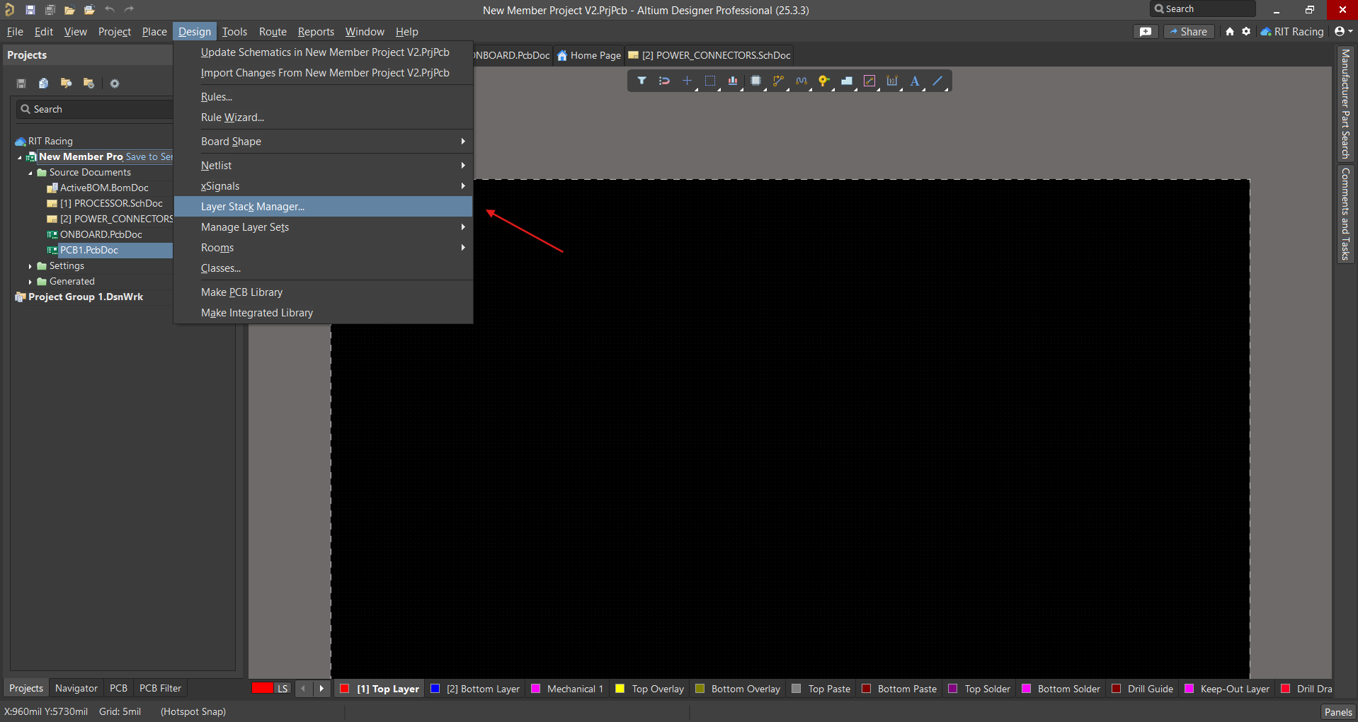
To access the layer stack, navigate to Design → Layer Stack Manager.
-
The default layer stack on Altium does not have the ground and power planes. Instead, it just has two signal layers (in yellow):
-
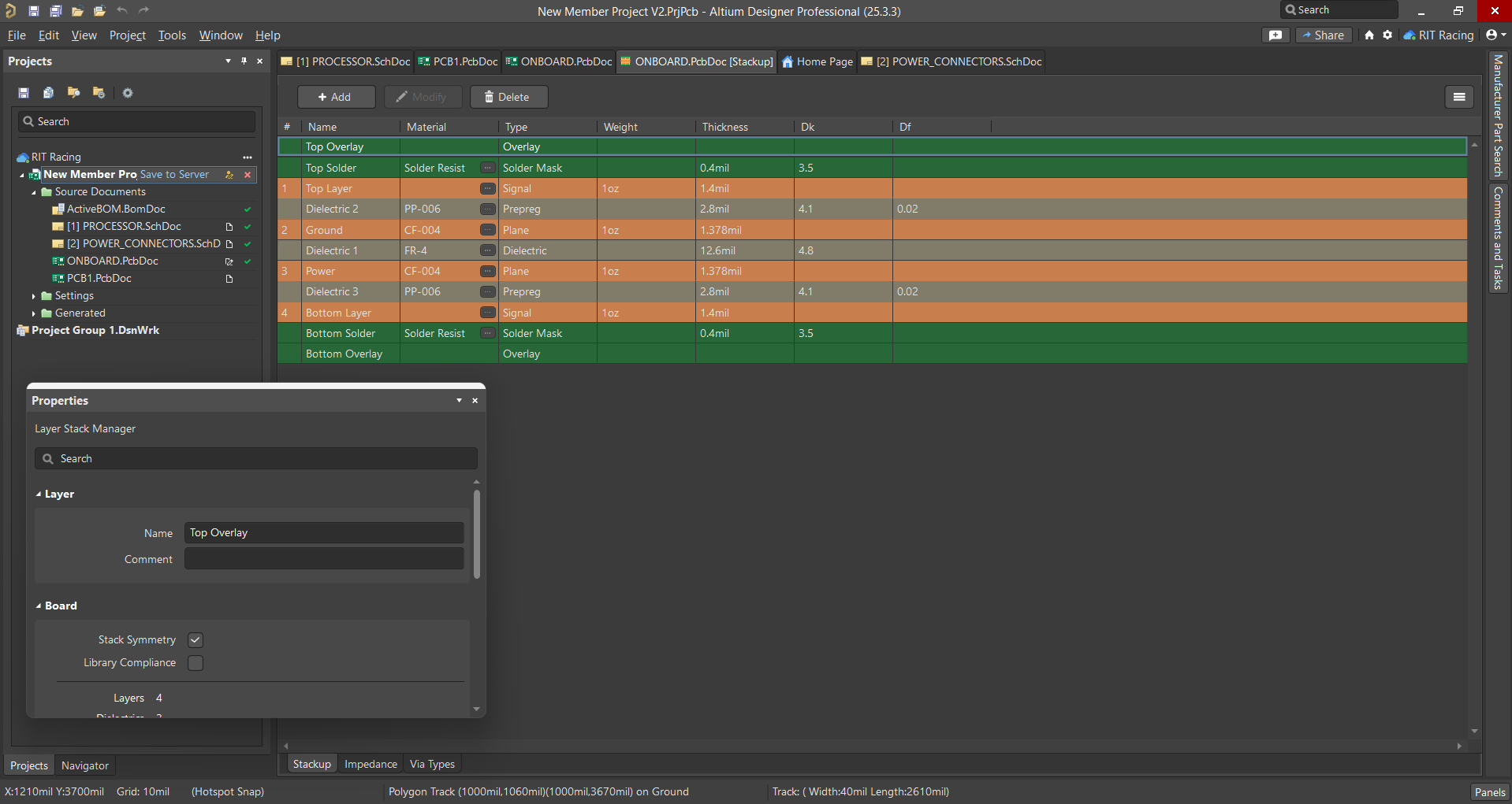
The configuration described earlier can be seen here in the New Member Board stackup. To create this, simply add and edit the required planes:
-
Once the layers have been set up, you can return to the main PCB document.
Components
-
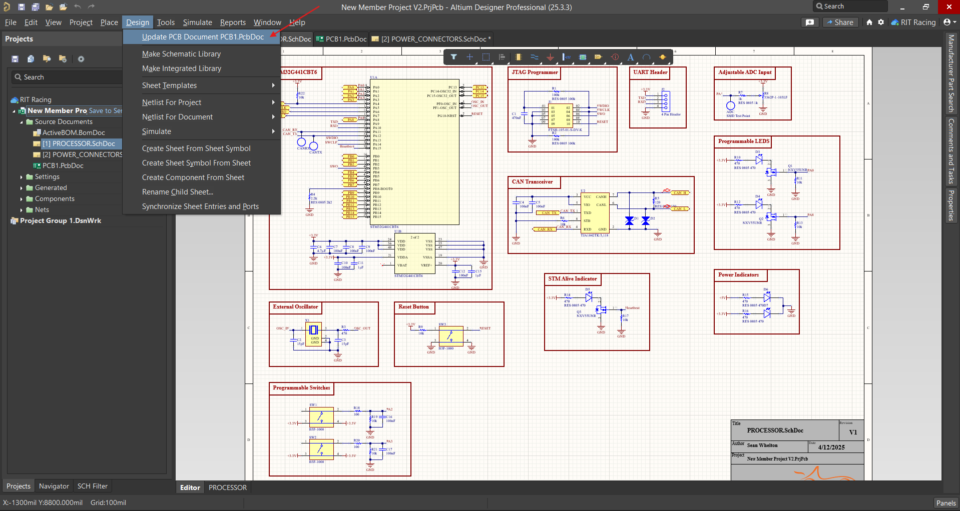
The schematic is used to initialize and update the components on the PCB. This can be done by selecting Design → Update PCB Document at the top.
-
A window will open with the list of components to be updated. The checkboxes on the left indicate whether a particular component should be updated based on the PCB. By default, these should all be checked.
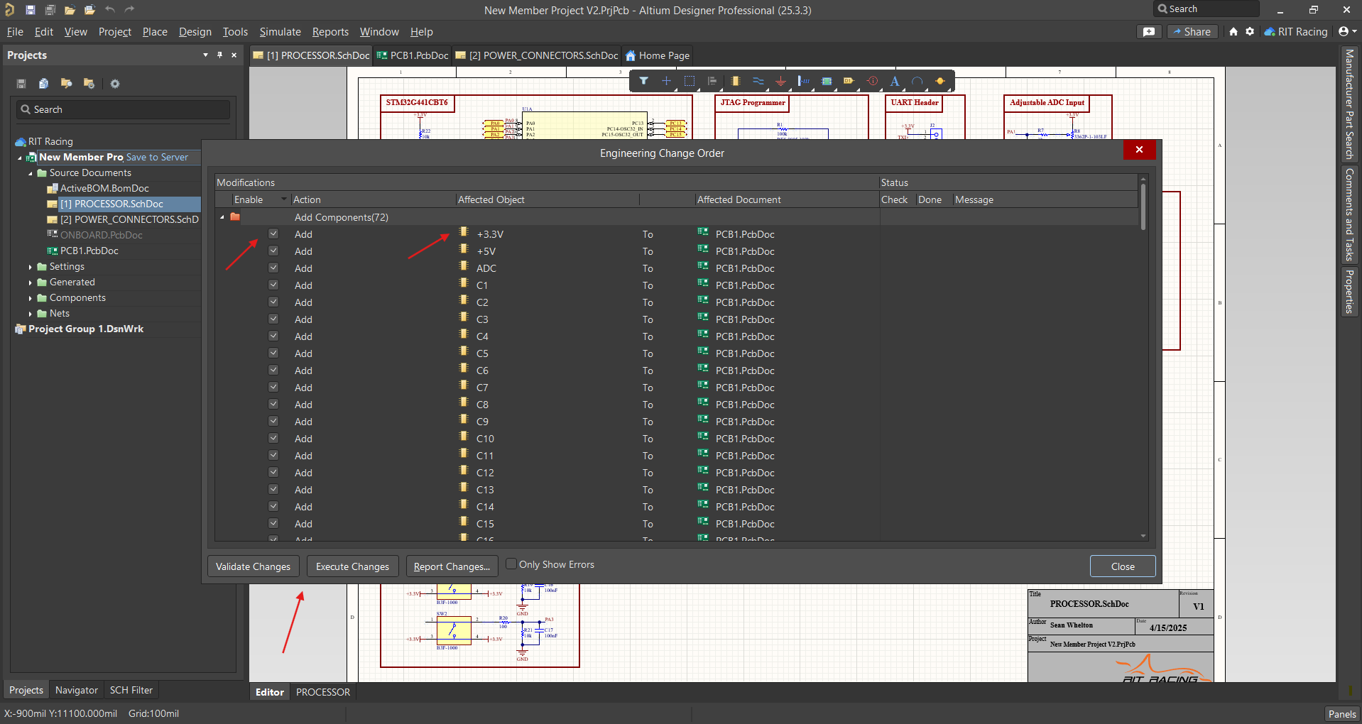
-
After confirming that everything is in order, you can proceed with executing the changes. The default footprints of each component will appear in an arbitrary position on the PCB. These are connected with light lines indicating the net.
-
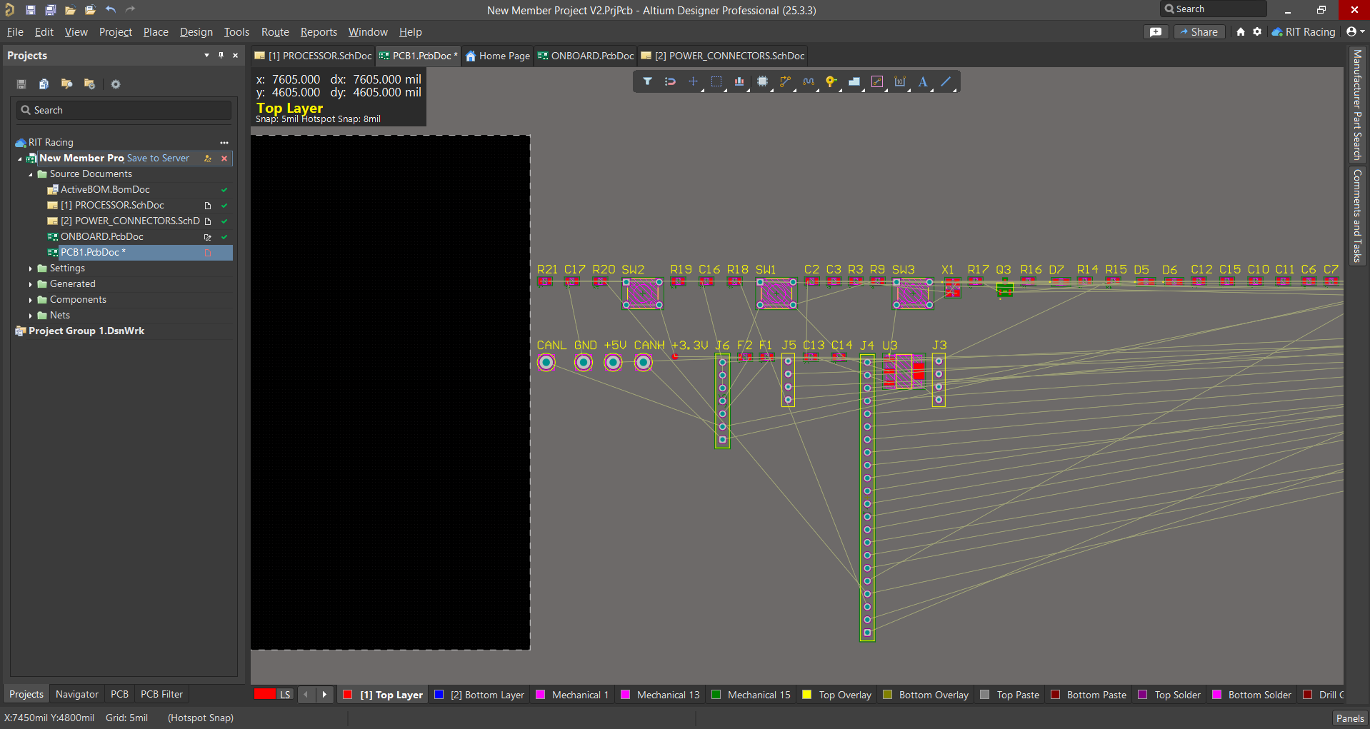
Bring the components onto the board by clicking and dragging them, and begin to lay them out.
There are a number of things to keep in mind when coming up with a particular layout, but the general idea is that the component positioning should be logical, with the nets and routing in mind.
Routing
There are a number of ways to route connections on a PCB:
- Trace
- Polygon pour
- Via (for connecting layers)
Trace
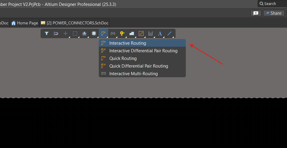
A trace represents a wire—the simplest connection between components. To draw a trace:
-
Select Interactive Routing from the toolbar. The short-cut for this is Ctrl+W (as with drawing a wire in the schematic). Optionally, you can adjust the settings for interactive routing to disable automatic rule-based corrections.
-
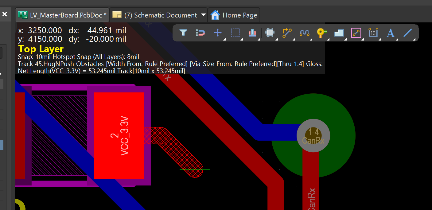
Click where you want to start your trace. If you start on a component, the trace will automatically inherit that component’s net.
-
Move your cursor to extend the trace and click again where you want the end point of that straight-line segment.
-
Press Esc to leave it there or continue by extending a second segment in the same way. Press Backspace to remove the last vertex.
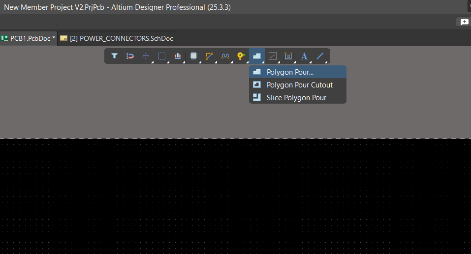
Polygon Pour
A polygon pour is a solid copper object, which has greater surface area than a wire. This can be beneficial for a number of reasons (e.g., lower impedance and better heat dissipation).
To draw a polygon pour:
-
Select Polygon Pour from the toolbar.
-
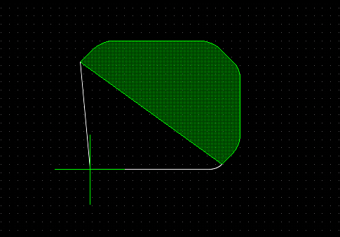
Click where you want the starting vertex to be.
- Press Shift+Space to toggle between different corner angle modes.
-
Move your cursor to extend an edge and click again to create another vertex. You can create as many vertices as desired and press Backspace to remove the last vertex.
-
Press Esc to complete the object. Ensure all corners are closed; otherwise, the polygon may not generate properly.
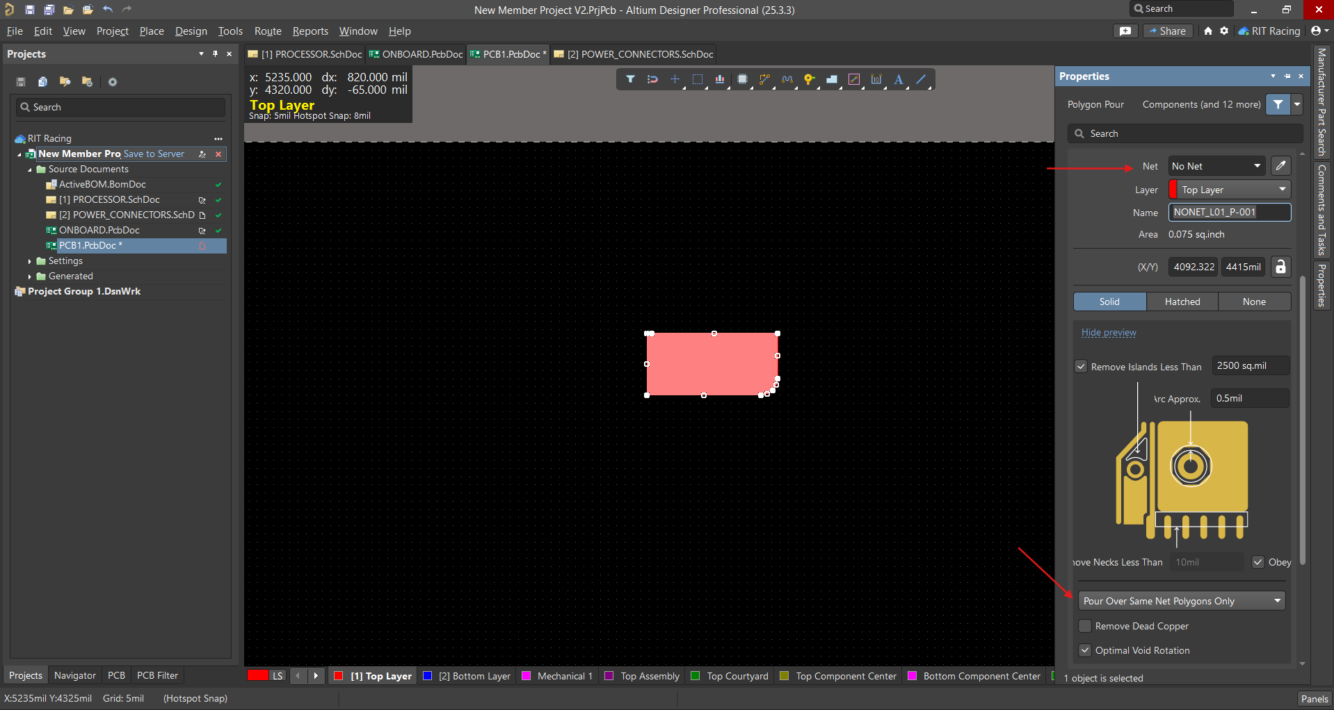
- To attach the polygon to a net, select the polygon and select it from the Net section of the Properties panel.
-
The Pour Over Same Net section in the Properties panel determines how the polygon interacts with other objects in the same net.
-
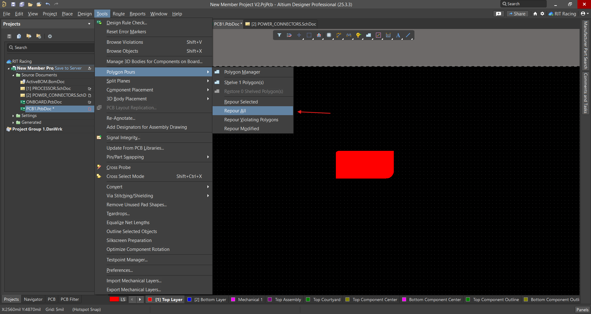
To ensure that the polygon remains intact after any modifications are made, enable Repour All at the top in Tools → Polygon Pours.
Via
A via is a connection between different layers of a board. There are 3 types of vias:
- Through-hole (1)
- Blind (2)
- Buried (3)
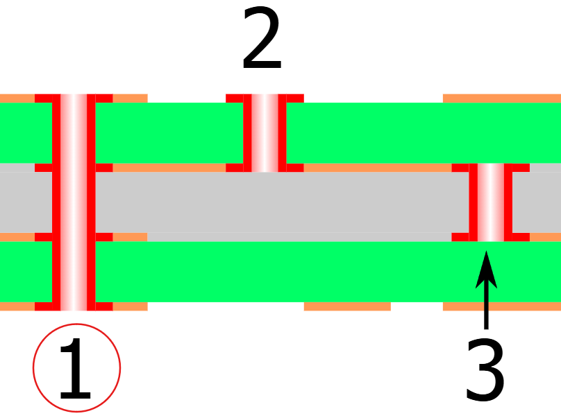
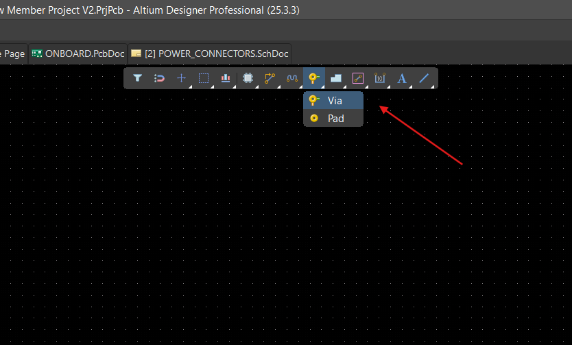
On the team, we exclusively use through-hole vias. To add a via:
-
Select Via from the toolbar.
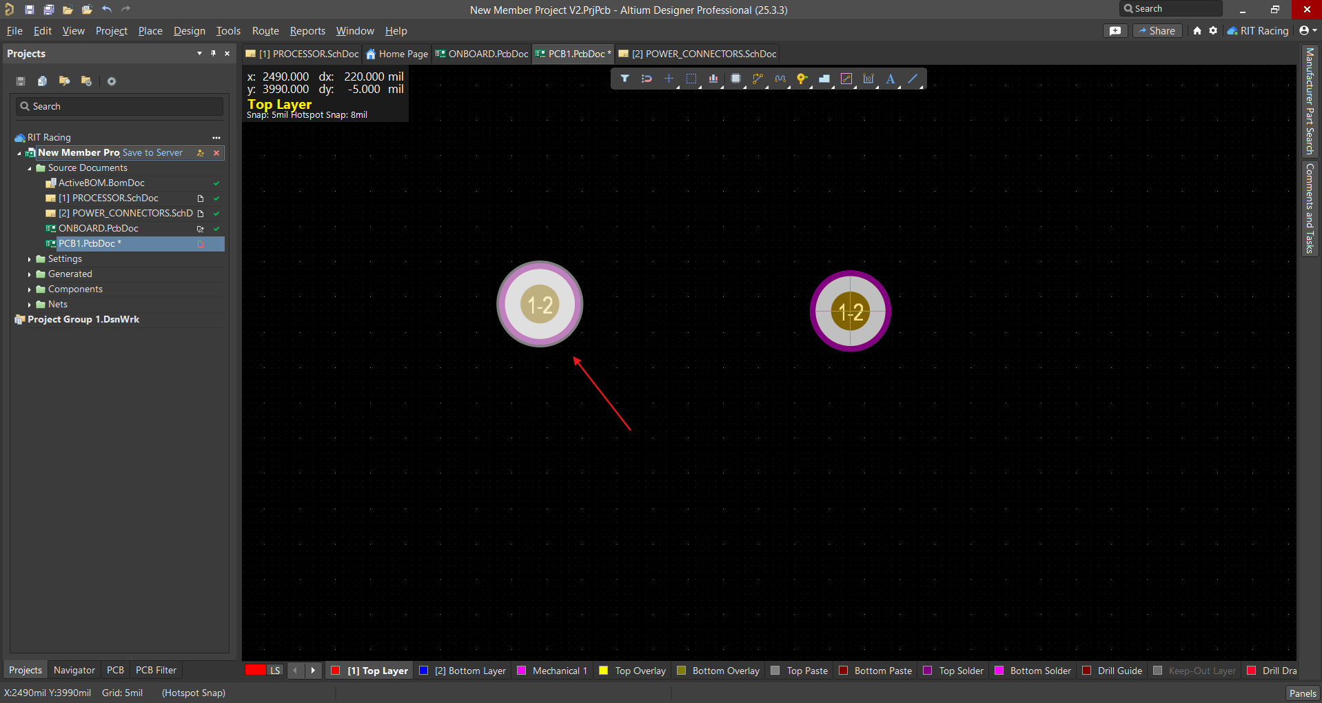
-
Move the mouse to position the via. You can press the Alt key to restrict vertical or horizontal movement (this may be useful for alignment). Click to place in the desired position.
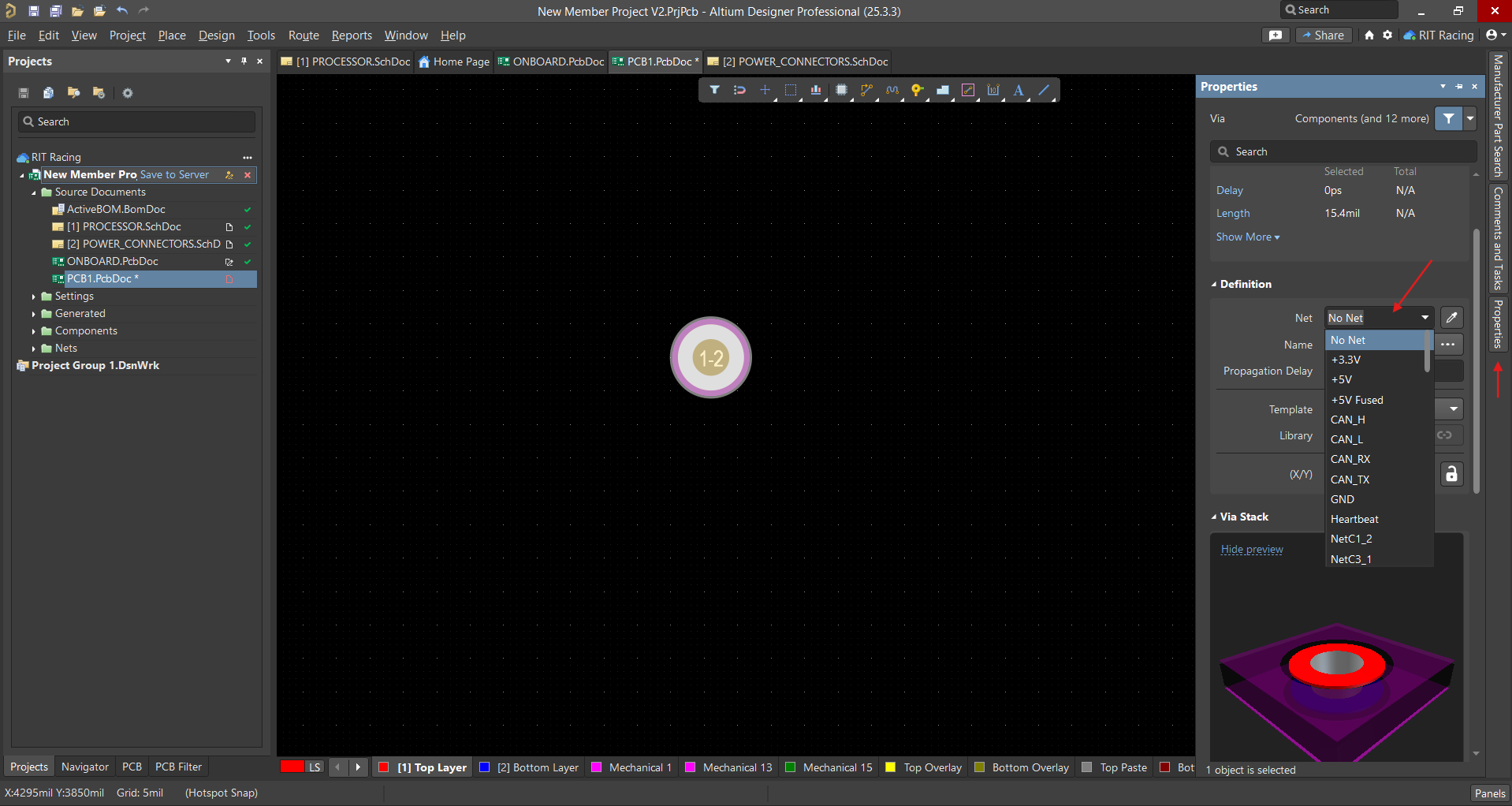
-
Assign a net to the via in the Properties panel.
-
Alternatively, vias can be auto-placed by pressing 2 while routing.
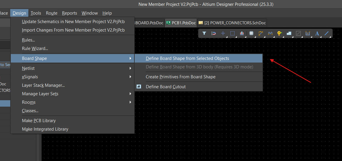
Board Shape
Defining the board shape is an important step in the PCB design process. The following shows an empty board, but this can also be done after placing components and completing routing.
One way to define the board shape is by using a predefined outline:
-
First, draw the shape of the board as you like using primitives (i.e. lines, arcs, shapes) on a mechanical layer.
-
After ensuring the shape follows the border region you intend, go to Design → Board Shape → Define Board Shape from Selected Objects.
-
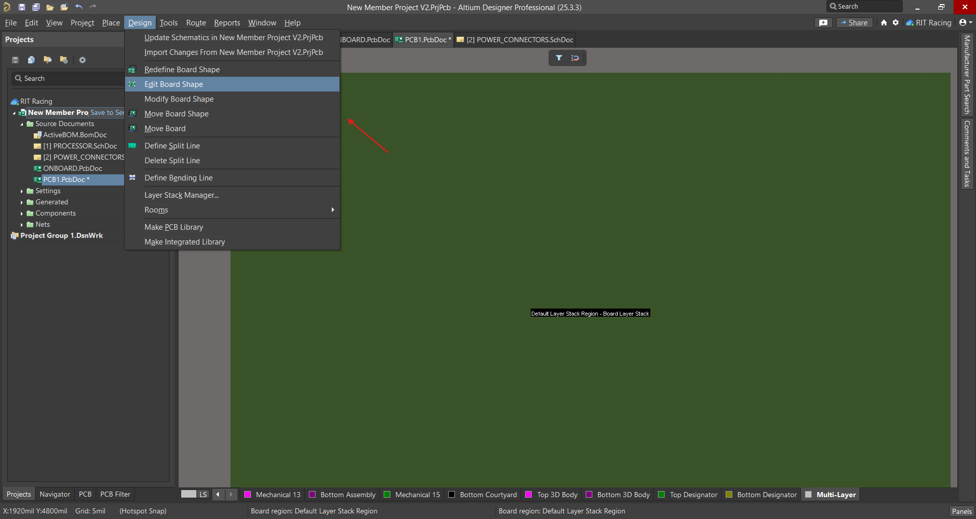
Alternatively, you can define/edit the board shape by pressing the 1 key, and going to Design:
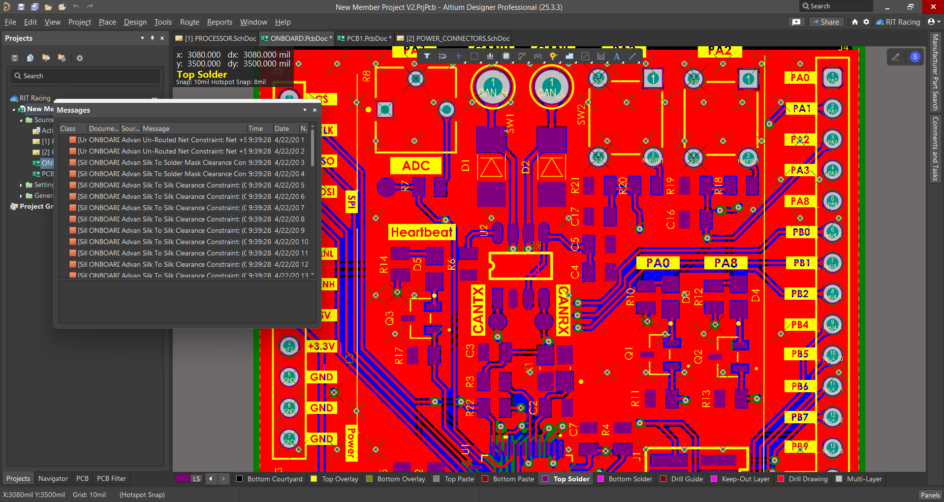
Design Rule Checker
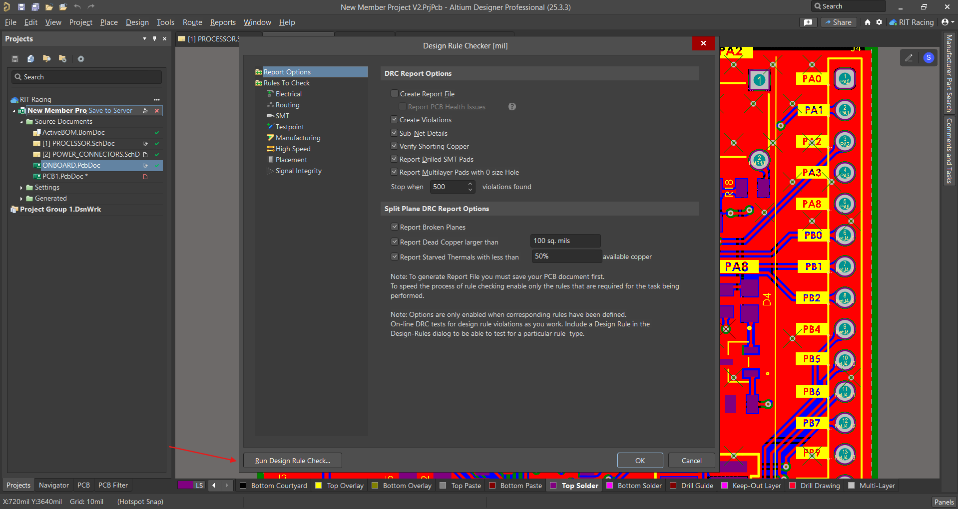
To confirm that the design conforms to rules, you must do a Design Rule Check, which checks all elements of the PCB against the enabled design rules. This includes constraints like minimum trace width, clearance, and routing violations.
-
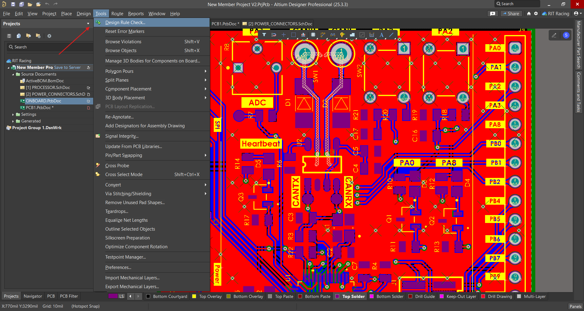
Go to Tools → Design Rule Check.
-
You can edit settings as necessary, both for the report file and the rules being checked.
-
Run Design Rule Check.
-
A window should appear with messages describing any violations.
Silkscreen
The silkscreen is a layer of the board that contains labeling and graphics. These are not linked to the circuit itself, but provide important information about the board like the name and revision. On Altium, this is the Top and Bottom Overlay.
Labels
-
Text can be added to the silkscreen by going to the toolbar and selecting Place → String.
-
The + and - keys cycle through which layer the string is placed on.
By default, all components on the PCB are labeled with the component designators, the formatting of which can be modified. In general, a few specific changes help improve readability and consistency:
TrueType Text
- Select one of the labels and right-click.
- On the menu, select Find Similar Objects and OK. This should select all of the component labels.
-
In the Properties panel, select TrueType in the Font section.
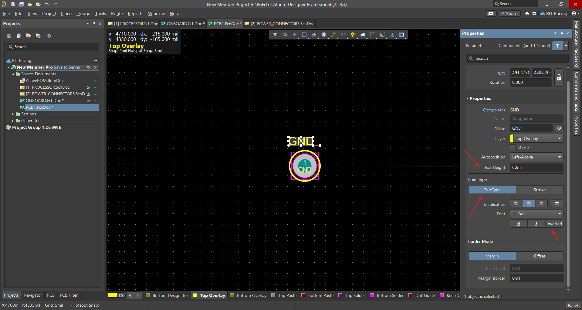
-
Depending on the use, you may choose to make the text inverted (particularly for the text you want to make stand out).
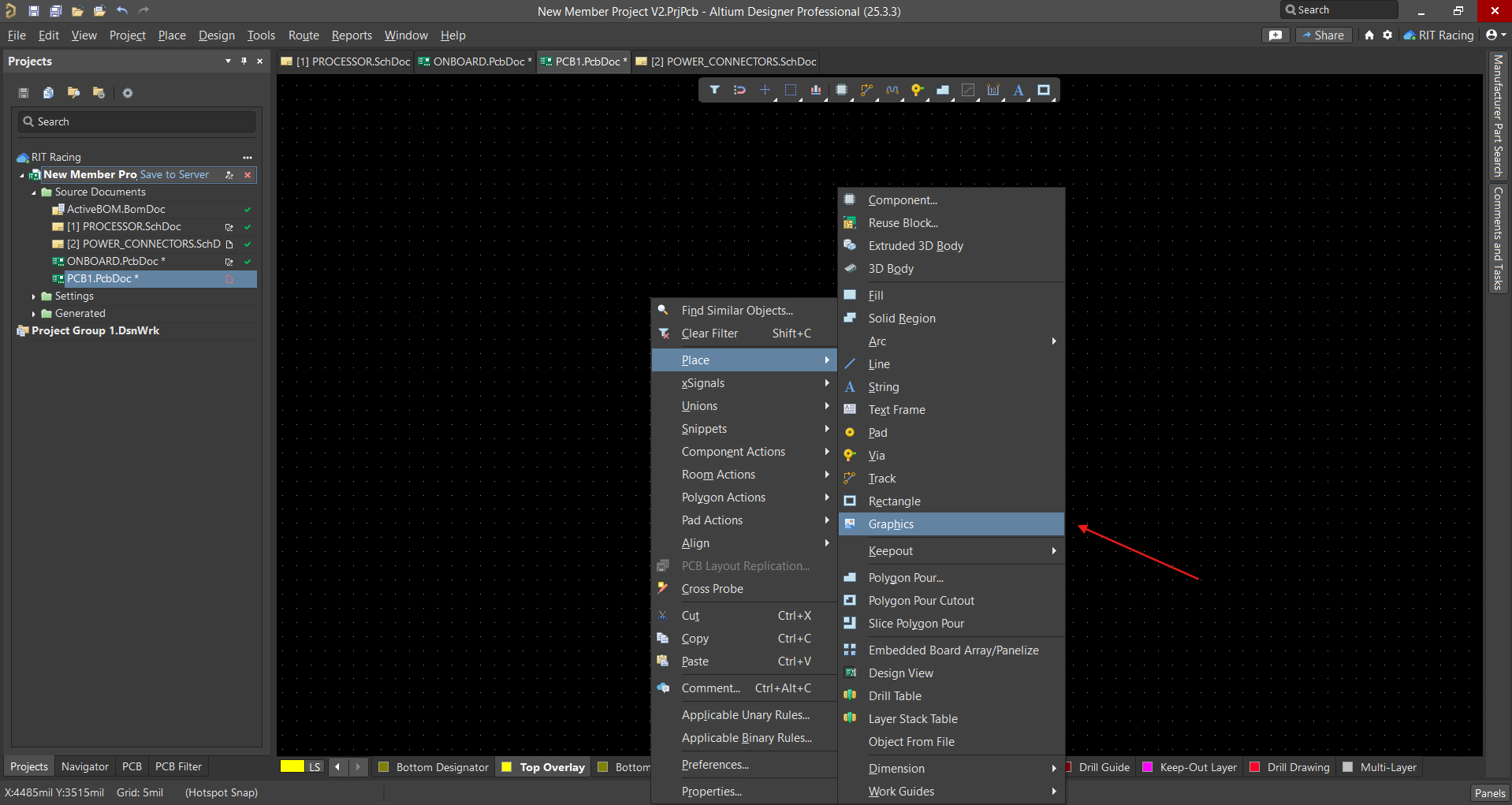
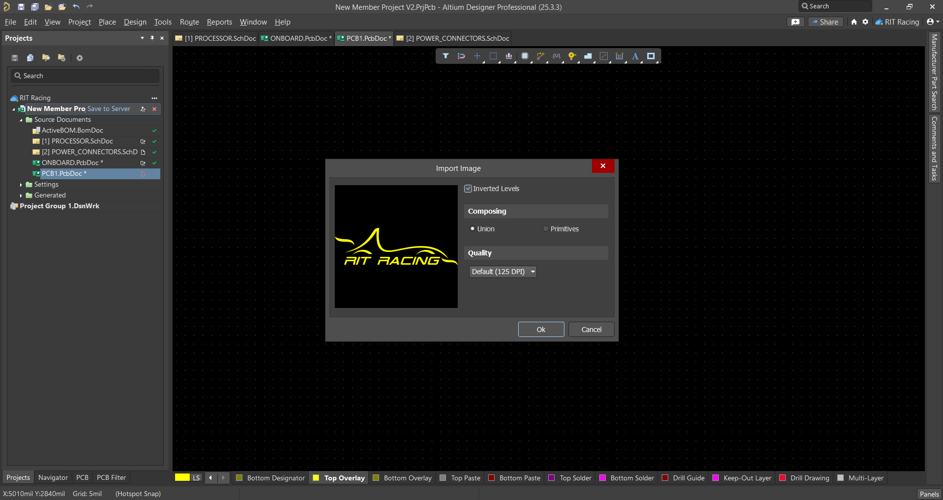
Images
Most boards will also require graphics, like the RIT Racing logo. Files for commonly used graphics can be found on the Silkscreen Files page.
- Download the desired image if you don't have it already.
- On the PCB document, select the appropriate overlay layer (Top Overlay or Bottom Overlay) before placing the image.
-
Go to Place → Graphics.
-
Drag to select the space you want the graphic to occupy.
-
A window will open showing your file system. Select the image you want to use.
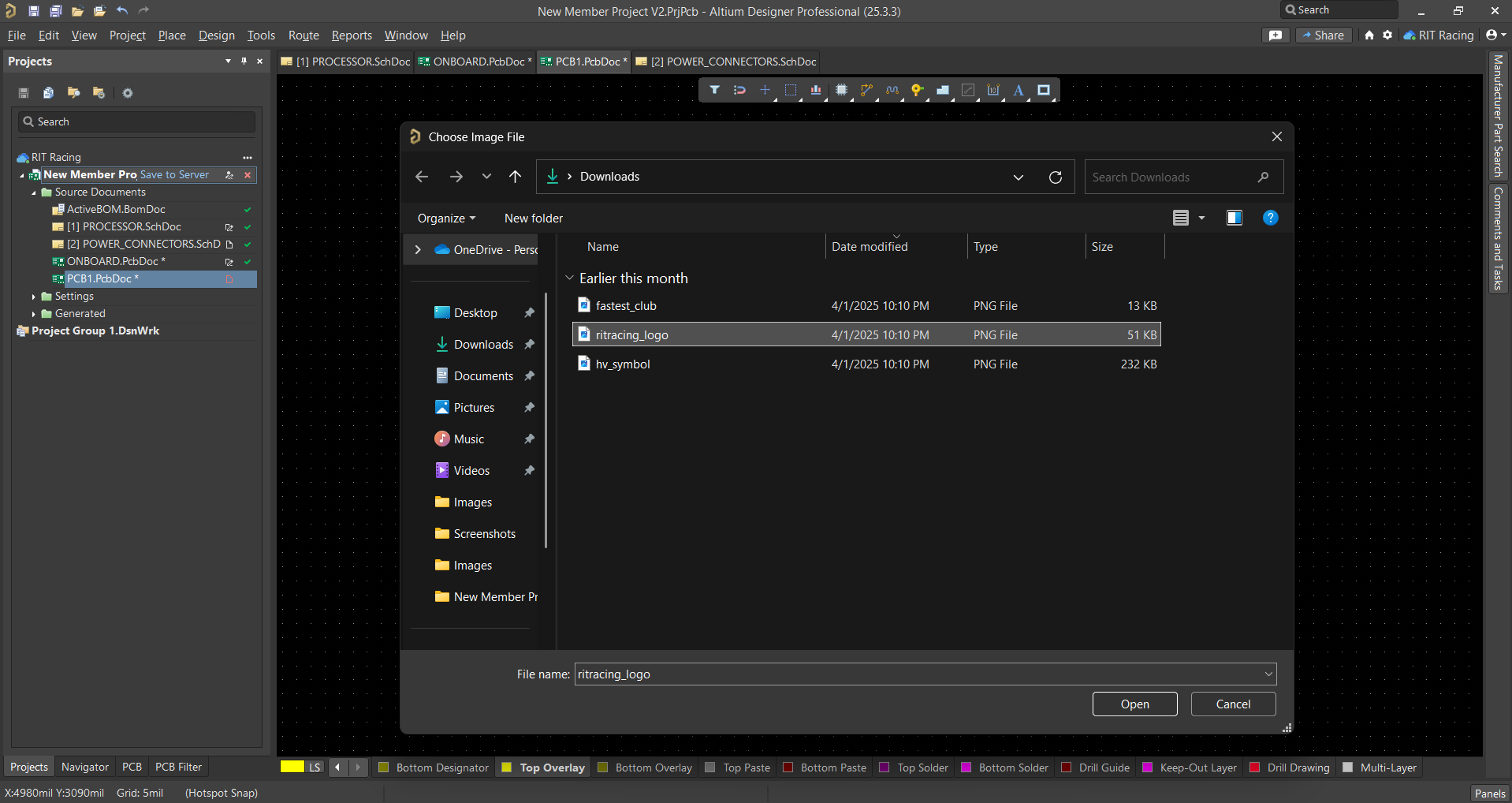
-
The graphic should appear as part of the silkscreen.
Further Reading
This is just a brief introduction to PCB design.
For more specifics and questions, look at the Resources page, where you can find links to explore all of Altium's features and capabilities as well as general knowledge about PCBs.