Schematic Basics
After setting up your project, you can begin designing the schematic. This acts as a blueprint of the circuit. Once it's created and validated, Altium can use it to populate and update the PCB with components.
Adding Symbols
-
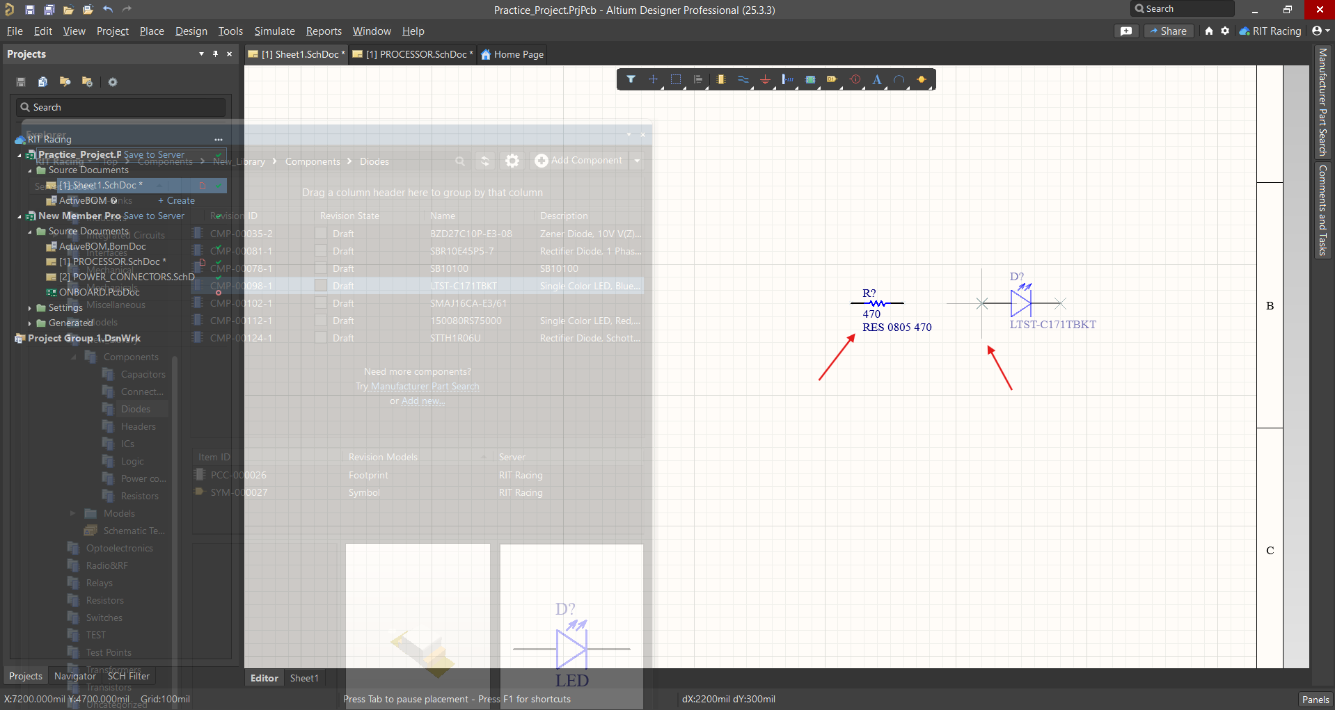
Choose a part from the components library.
-
Right-click on the part and select Place. If the component has multiple parts, you will have to choose one.
-
The symbol will appear translucent. Position it by hovering the mouse over the desired position and click to place. Right-click or Esc to cancel. After placing the symbol, rotate it by selecting it and pressing Space.
-
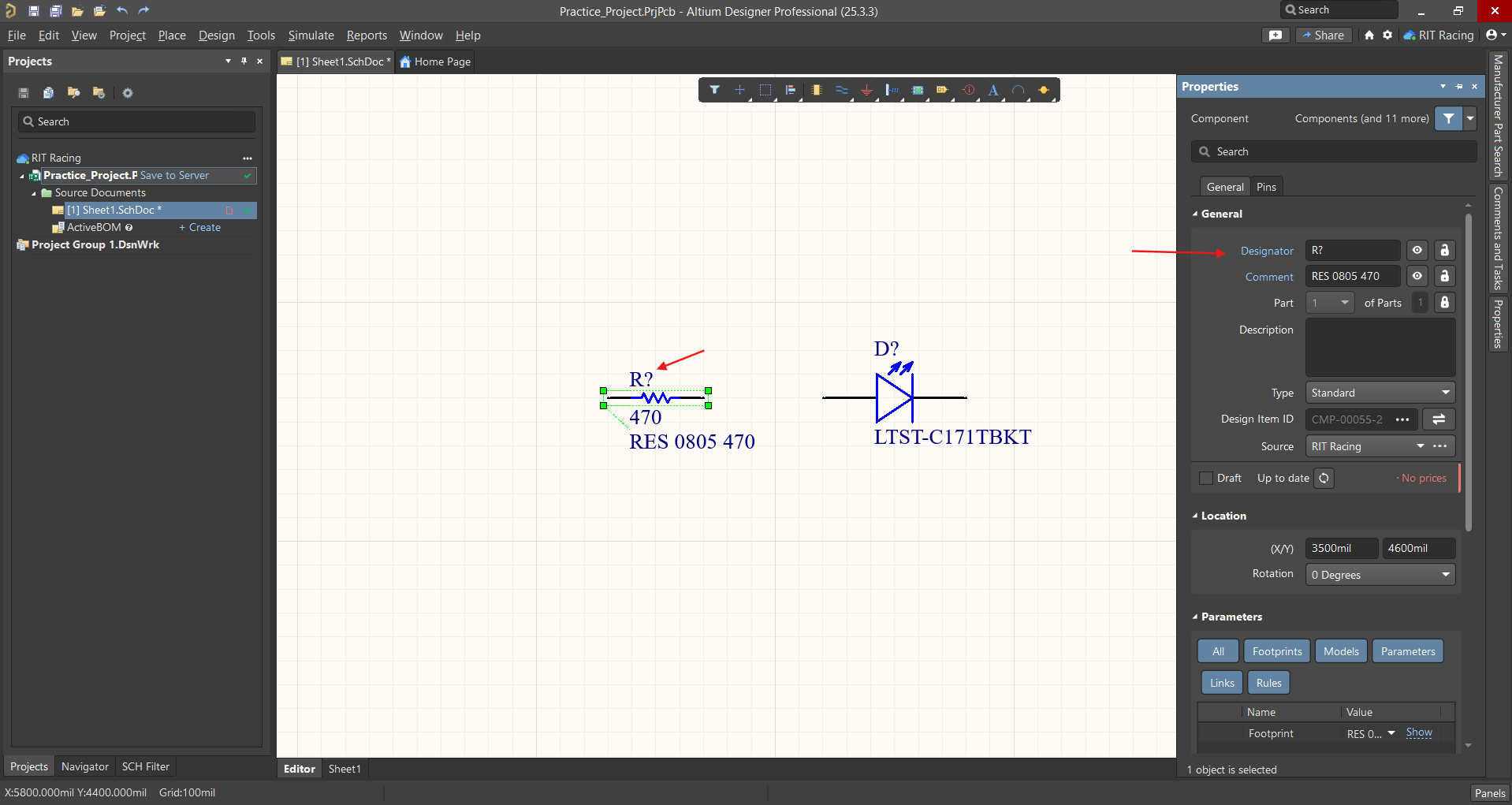
Once placed, you can select the symbol and go to the Properties panel to access details.
Annotating the Schematic
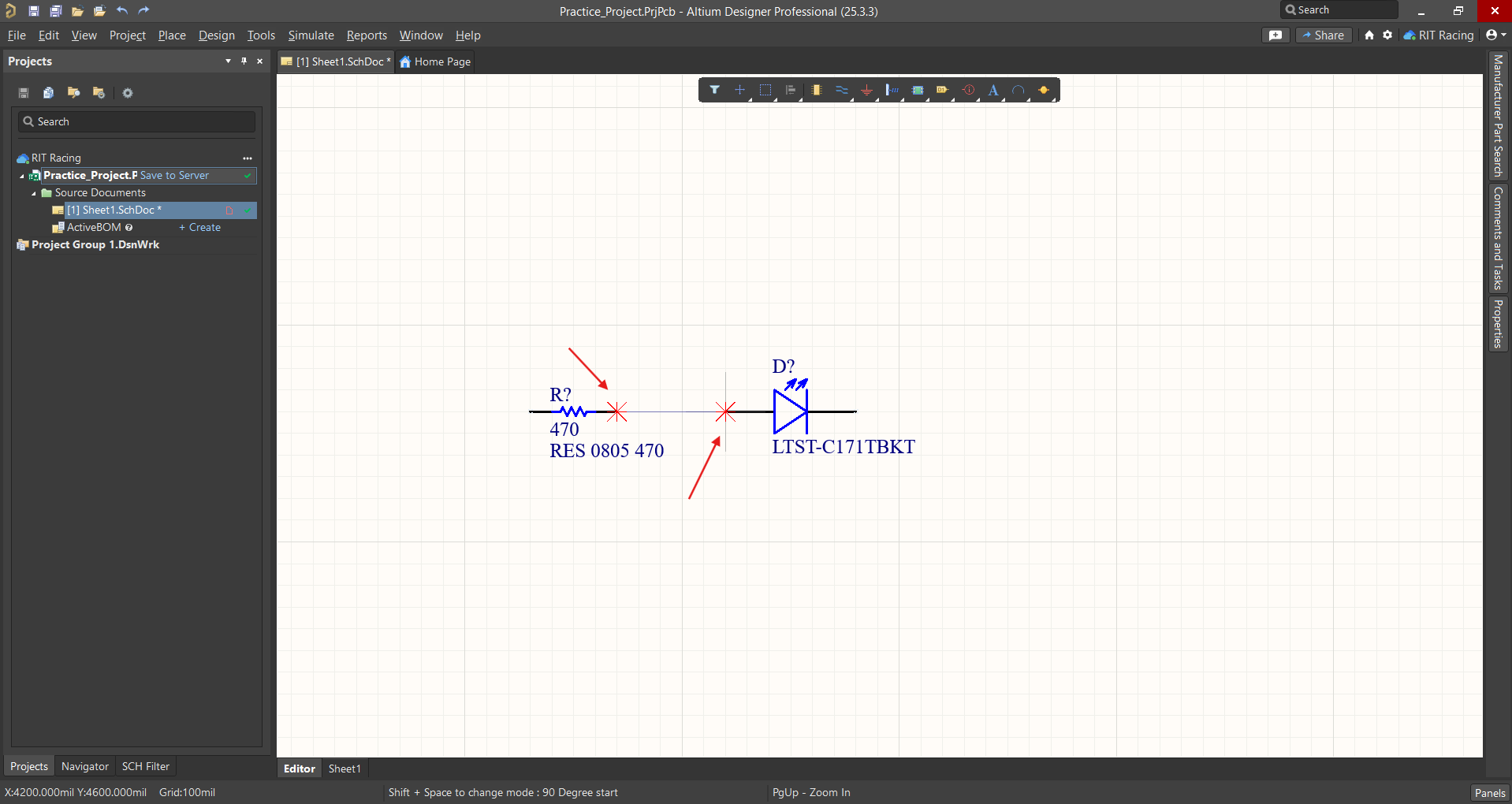
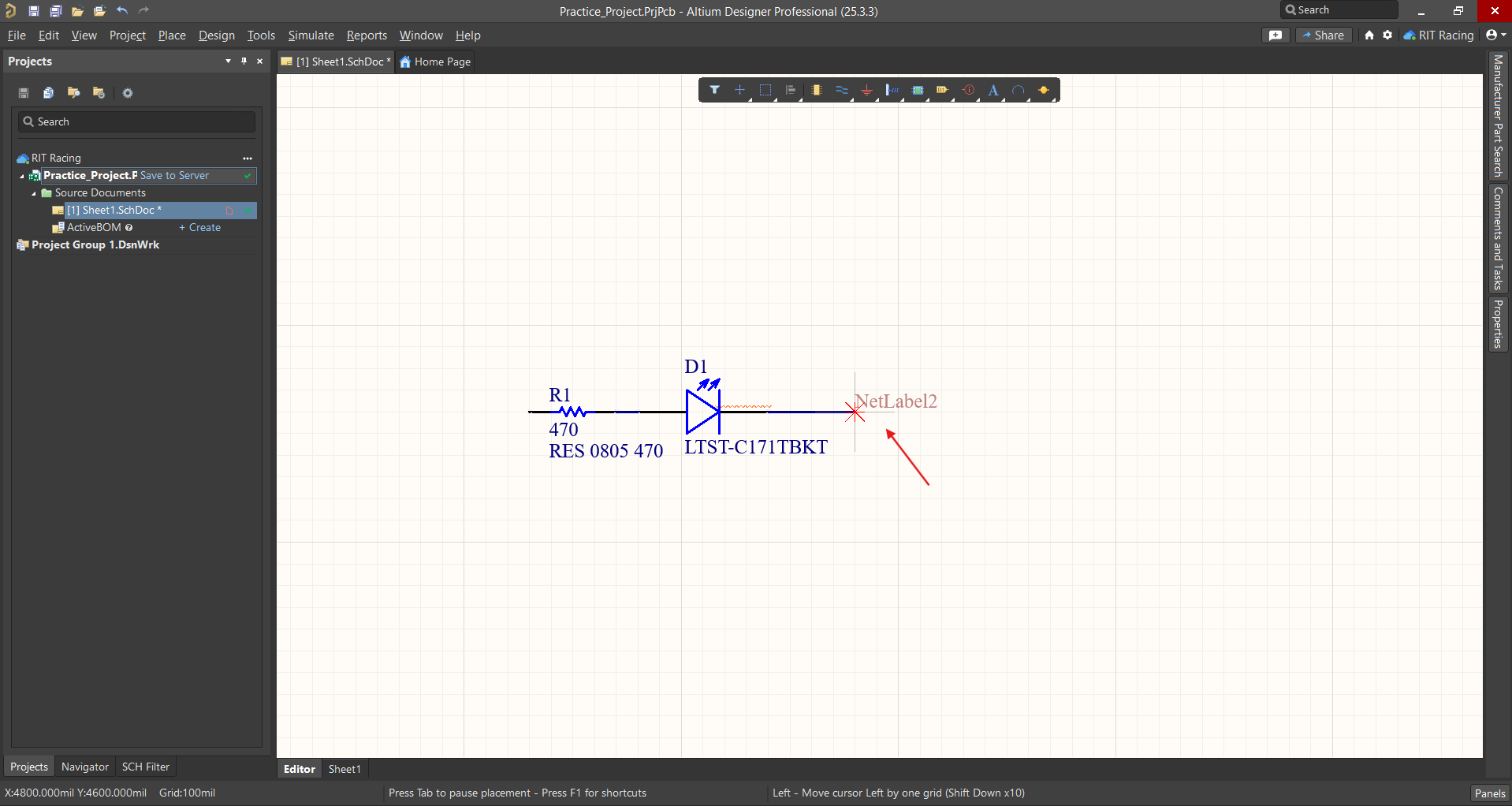
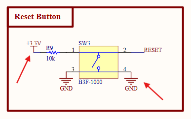
A component is labeled using a designator which can be edited in the Properties tab. The prefix (letter) is based on the type of part, and the number distinguishes it from other components of the same type.
These are some common components:
- R - Resistor
- C - Capacitor
- L - Inductor
- K - Relay
- Q - Transistor
- TP - Test Point
- U - Integrated Circuit
To automatically annotate components:
- To to Tools → Annotate Schematics Quietly.
- To undo or redo the annotation, you can go to Tools → Annotate Schematics which allows more fine-tuned control.
Alternatively, components can be manually batch-annotated by type:
- Right-click on any one placed component (e.g., a resistor).
- Select Find Similar Objects.
- In the window, set Designator and Kind as Same.
- Click OK — this selects all similar parts (e.g., all resistors).
- Go to Tools → Annotate Schematics Quietly.
Connecting Parts
Components in a schematic are connected together with a net. This can be indicated either by physically wiring them together or assigning a net label.
Wire
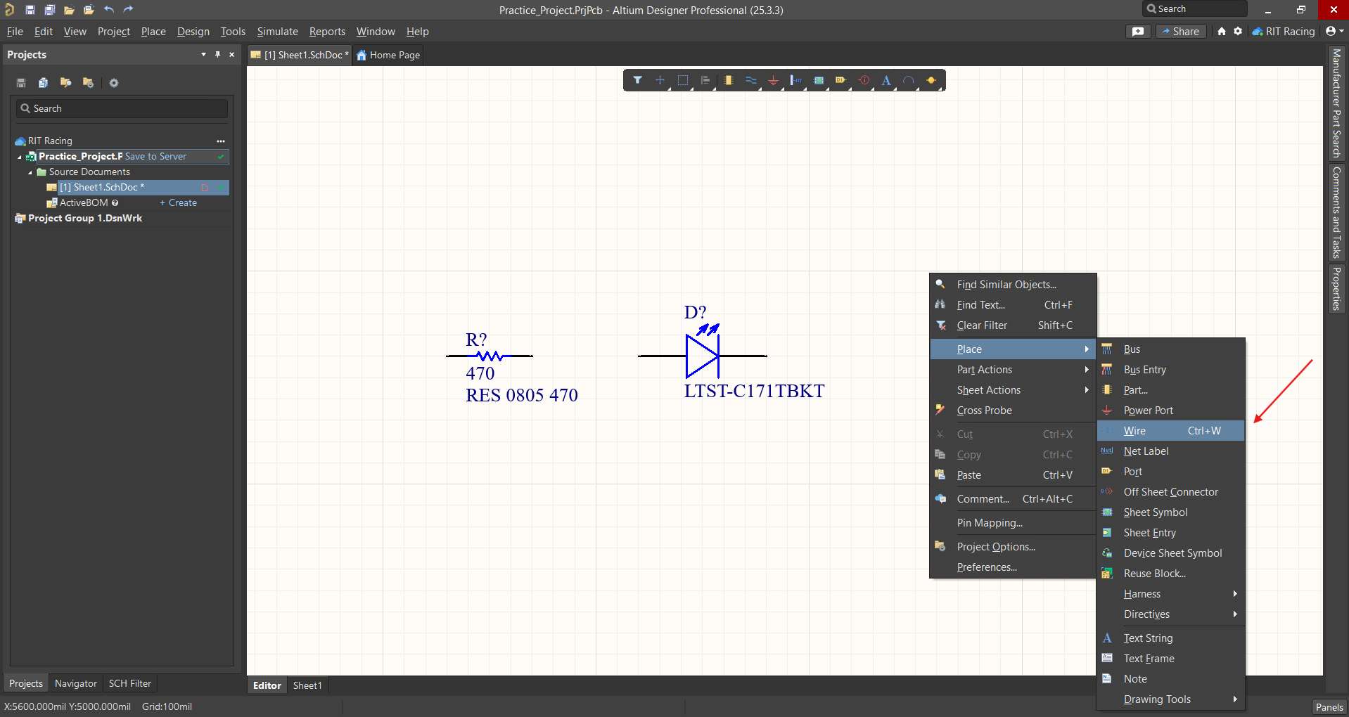
A wire can be drawn by right-click and select Place → Wire, or more easily, with Ctrl+W.
Hover to position and click at the connecting pin to attach. Then click on the other component where it should connect. The wire adjusts when the component is moved.
Net
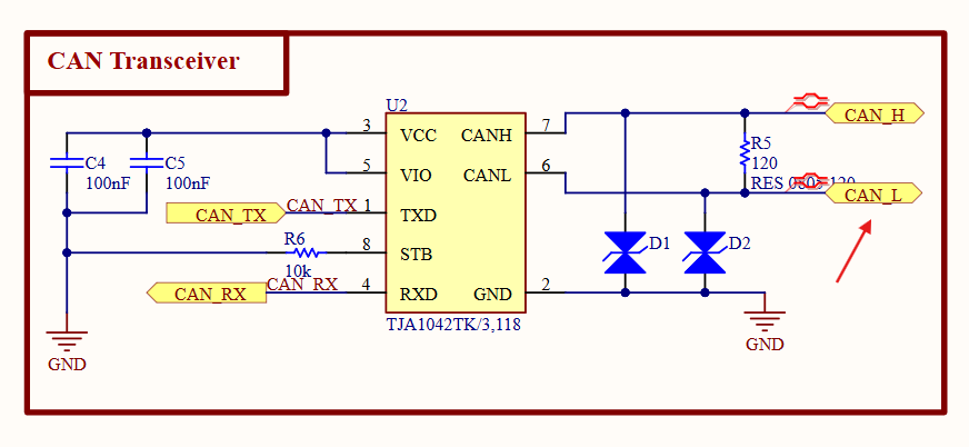
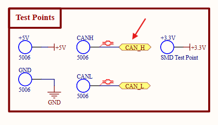
All connected components are part of the same net. In a schematic, you can indicate that a component is part of a particular net, even if it appears separate, by placing a net label.
Connect a short bit of wire to the desired pin. Then, similar to placing the wire, right-click and select Place → Net Label. This should be connected to the end of the wire, and the text edited to indicate which net it is a part of.
Port
A port makes a connection between multiple sheets of a schematic. The name of the port on one sheet corresponds to the name of the port on the other sheet to which it connects. It is placed the same way as a wire or net label.
A power port specifically indicates a connection to a power or ground net.
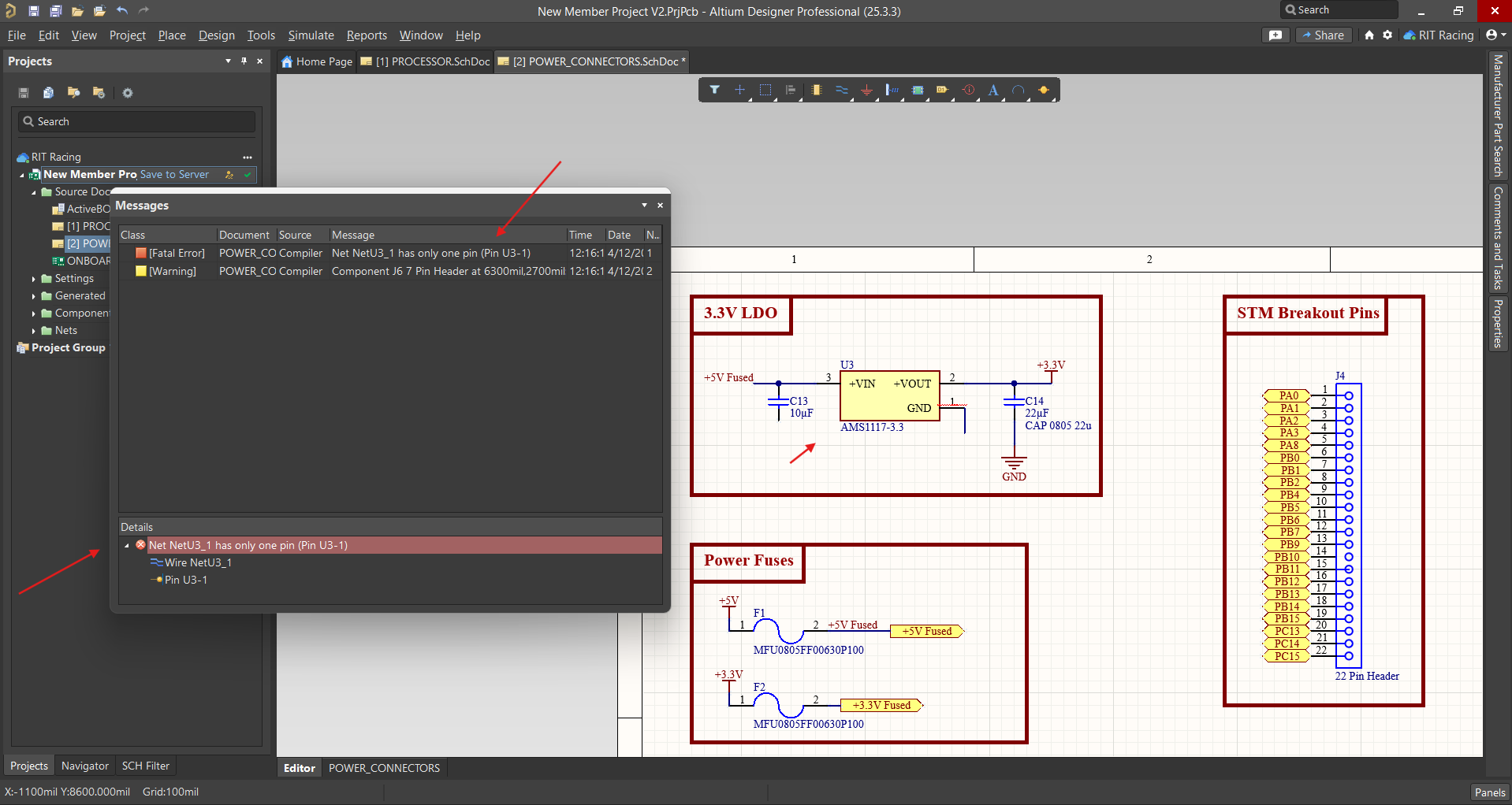
Validation
Once the schematic is complete, it needs to be validated to check for any errors. Validation must be completed before generating the PCB layout.
To do this, go to Project → Validate Project.
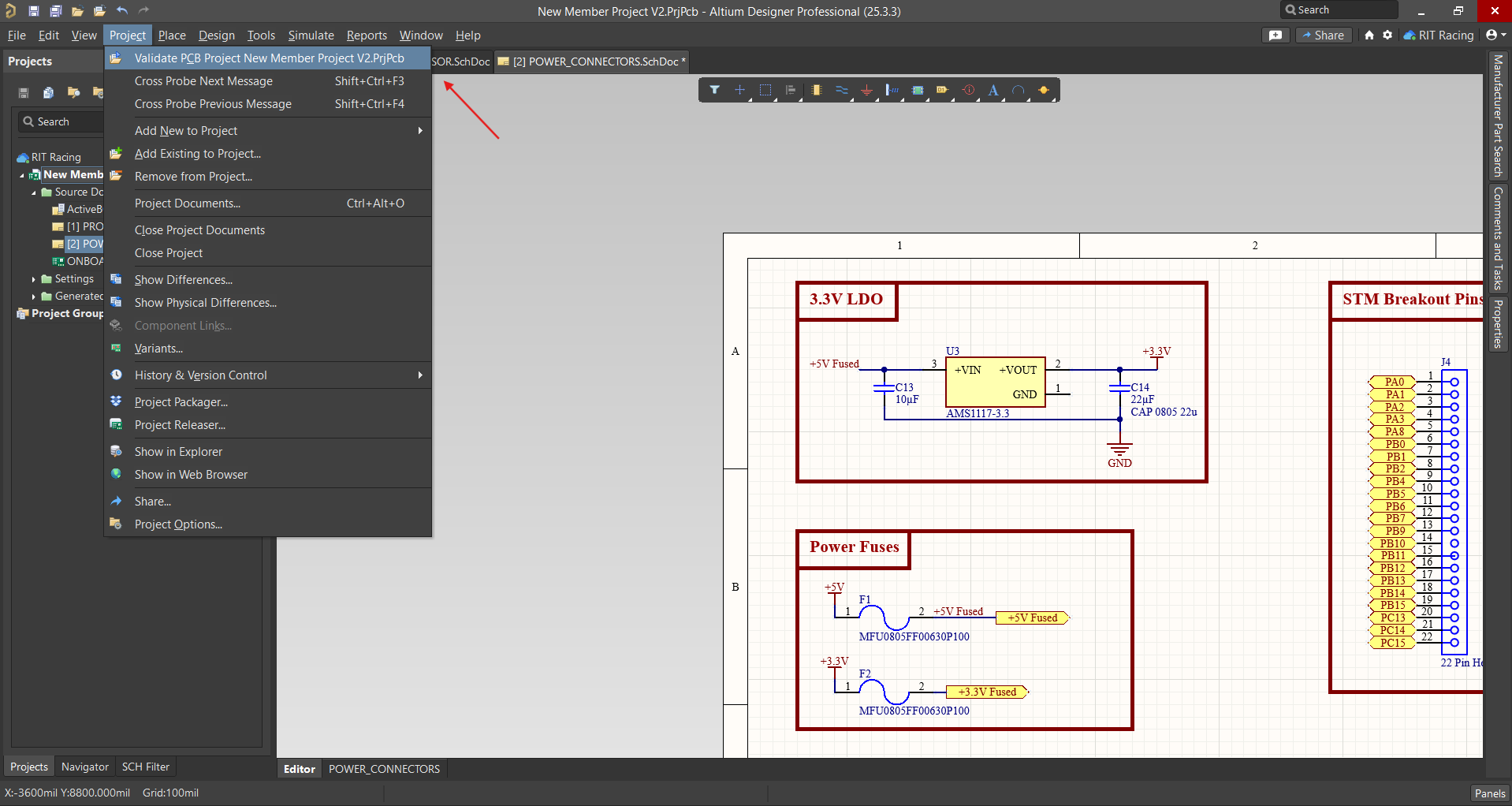
Errors or warnings in the schematic design will appear in the Messages panel. Some can be ignored, but others indicate issues that need to be resolved. In this example, a wire has been removed to demonstrate the resulting errors that must be corrected: